Imprint Stamp Fabrication Services

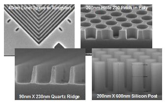
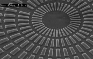
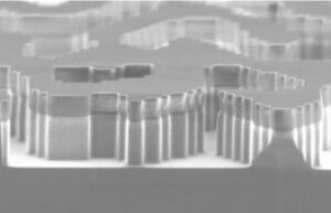
Benchmark Technologies’ highly experienced staff possesses a unique set of core competencies in the areas of imprint stamp fabrication. For almost 20 years Benchmark Technologies has been providing services to develop and manufacture imprint stamps. We work closely with our manufacturing partners to provide quartz and silicon imprint stamps. Typically we use electron beam lithography and reactive ion etching to produce stamps that meet the needs of our customers. Our stamps are used in a number of areas including micro-fluidics, optical gratings.
Our experience in this area has lead us to develop multiple manufacturing partners that can be leveraged depending on the need of each customer project. For small areas with very small features, e-beam lithography may be the best solution. In other cases with larger features and stamp areas, laser lithography may be an acceptable and lower cost alternative. In still other cases the most cost effective way to produce large area stamps may be optical lithography using wafer scanners.

At Benchmark we delivered on projects using all these lithography approaches with stamp sizes from 10mm X 10mm to 300mm diameter wafers, and features as small as 40nm. If you have an imprint stamp project that we can help on, please contact us.

